Please read this first before continuing to the project:
Dear fellow hobbyists,
Recently it has come to my attention that someone in Brazil has started a pirated production of ZXpand clones. I was told this person made “assumptions” that ZXpand were a public domain project and that he found the ZXpand bootloader and firmware on my website. As per my project description below anyone can clearly see that there is NO bootloader nor firmware on my website of the ZXpand, the ZXpand is NOT public domain.
So I will state it clearly: The ZXpand firmware and design are the property of Charlie Robson. The ZXpand firmware is his hard work of years which he generously invested in this complex project. The ZXpand firmware and design may not be used for anything unless Charlie Robson gives you permission to use it.
The ZXpand firmware can’t be downloaded anywhere, especially not on any website of mine. Anyone claiming it is, is simply lying and inventing things to get out from underneath the responsibility of proper and legal conduct.
Furthermore I would like to comment specifically on this unauthorized ZXpand clone production in Brazil. I was deeply saddened by this news. Perhaps in this day and age it is to be expected, but still, even in the relatively small ZX community to find this happening was quite disappointing to me…. In my opinion it is not only rude, inappropriate and illegal to run such a project, it is also plain and simply stealing of the intellectual property which belongs to Charlie Robson as you can clearly read from my project page. It is his hard work which is being stolen here.
From now on, if you contact me for this design, I will only pass along any gerbers if I can notify Charlie Robson with your contact details.
And anyone who wants to build this project, I will state it again just as I have emailed any interested party before: get PERMISSION and the firmware first from Charlie Robson, under his terms before doing anything with these designs….
Thank you for your attention and please excuse this unfortunate but necessary interruption of your reading.
After finding the very excellent ZXpand interface on the internet in 2013, I was impressed when I discovered how professional this interface is and how much practical functionality it adds to a ZX81. It was created by Charlie Robson, also known as Sir Morris in the ZX community. Charlie had spent 7 years of hard work in his free time to develop, debug and perfect the ZXpand into the great addition for any ZX81 that it has become. The ZXpand is really the best thing that could be added to the ZX81 to make it much more fun and easier to use.
At that time I thought, how great would it be to have a ZX81 which has the ZXpand already included in a single PCB. And even better, if that PCB could fit inside an original ZX81 case! I was interested in a new ZX81 project to do, so I started looking into this possibility. Using some SMD components like in the Micro-ZX81 project, this certainly seemed like a viable idea.
In march 2013 I contacted Charlie and he has been very kind to assist me with schematics of the ZXpand and provide me with all the helpful information that I needed to be able to integrate the ZXpand into my existing ZX81 Issue 4 design.
He also took the time to answer several questions which popped up during my prototyping and debugging phases.
I want to thank Charlie once again for all his help. Without him, this project would not be possible!
I have integrated the following functionality into the design of this project:
– ZX81 Issue 4
– ZXpand interface
– AY-addition of ZXpand
– second AY chip, which means a total of 6 audio channels available
– power switch (yes, finally! 😉 )
– reset switch
– BIOS toggle switch to choose between original ZX81 and ZXpand enhanced ROM
– 4 LEDs for indicating: power, ROM mode, ZXpand’s drive activity and error led
– audio amplifiers with trimmer adjustable volume level
– active tone control circuits(bass and treble adjustment by PCB trimmers)
– expansion connector which includes important ZX81 internal data and timing signals
For details regarding the ZX81 Issue 4 and how I arrived at this design, please read the ZX81 Issue 4 page which also includes the sources of the project. This page is intended only to document the additions, and the project itself.
The final PCB design is of a larger form factor than the original ZX81 PCB, however I have made measurements and did some fitting which confirmed that this PCB indeed can still be mounted inside an original ZX81 case. This project has become a super compact ZX81 with SD-Card storage and 6 channels of chiptunes music capability. What more can you want? Well, perhaps some colours such as seen in the Chroma interface. But I really can’t fit that into the ZX81 case anymore I think. 😉
For this project I used a scope to examine the AY sound signals on my experimental prototype and finetune all the audio circuits. I found that the AY chips can benefit a lot from some opamp stages for amplification and from adding some active tone control which can help to enhance the sound to the user’s preference. Further details can be seen in the schematics.
Power considerations
During my testing of the prototype assembly I noticed some audible power supply interference from the zx81 circuits. This is probably related partially to the way my prototype assembly was powered and how the power was being distributed across several PCBs of which several were veroboards. Certainly not ideal, but I only built the prototype in order to prove the design, after which I will not use it anymore. After I discovered that the audio circuits were influenced by interference, I experimented with some coils and capacitors to try to filter the power supply going into the AY chips and audio circuits and make the sound more clean. The results were varied but I am keeping the options open in the layout. Only after building the first real PCB of this project I can determine if any of these filter circuits are necessary, or if perhaps some different components will be needed to keep the audio clean. In the schematics I assumed a somewhat worst-case scenario where I will need some coils and capacitors etc to separate and stabilize the audio power. In the final design, perhaps the board will even need almost no special power filtering at all. In the PCB design I considered the audio circuits as much as possible by using wide power traces and keeping the audio power traces as short as possible from the power entry point on the PCB. I have kept the audio power lines and ground planes completely seperate on the board, just in case. Additionally, I paid attention to adding as many audio-ground surface planes as possible around the audio opamp circuits and connecting critical parts of audio circuits which might suffer from interference with wider traces in order to decrease the resistance of these traces. Less resistance means less interference from neighboring signals. There are already various big improvements in the PCB design compared to my prototype and I am hopeful it will result in clean sound. I will report my findings as soon as I can test my first PCB. In the very worst case, a seperate power input can be wired to the audio power lines, but I am optimistic that nothing that drastic will be necessary. 🙂
About the modified ZX81 ROM
For the ZXpand to be able to function, it was necessary for Charlie to modify the ZX81 BIOS image, otherwise the necessary code would not fit into the very limited ZX81 ROM address space.
In order to provide 100% compatible BIOS code, I have decided to include BIOS toggle switch circuits into the design. I did some interesting experiments with different types of circuits to help to making switching the BIOS very smooth and contact dender free, until I had a perfectly functional toggle switch solution for this. It needs a few parts, but it’s worth it in my opinion to add comfortable toggle switching. I added a led to indicate which ROM is currently operational.
During my prototype tests I found that the screen in my design displayed some artifacts in it. This as it turned out was caused by the ZXpand enhanced ZX81 ROM code. So I experimented with several timing signals already present in the ZX81 Issue 4 display generation circuits, until I finally found a suitable solution for dynamically switching the original ZX81 ROM in place during display generation cycles, while keeping the ZXpand enhanced ROM enabled at other times. For an even more complete ROM compatibility with the original ZX81, there is the ROM toggle switch available that can select between ZX81 original ROM or ZXpand ROM mode.
After switching to the original ZX81 ROM, this computer will function the same as the ZX81 Issue 4.
About component usage
I remember reading some remarks about component usage on the internet. I want to briefly explain my own motivations regarding this aspect of schematic and PCB design. In the 1980s, indeed TTL components were expensive and reducing a single chip could result in lower production costs and power consumption. At the time, it made sense to do everything possible and spend many hours in the design stage to further reduce chip count. It is another kind of creative challenge during the schematic design stage. Those hours of chip reduction work could save a substantial portion in the total production costs. I remember hearing in some documentaries that Steve Wozniak of Apple was particularly talented in this field and could do amazing things with very few chips. It is an admirable talent indeed.
Since the 1980s, many things have changed. TTL chips have become very cheap. Chip size and power consumption have all reduced drastically. In these modern times, I don’t want to invest too much valuable time in reducing chip counts, but rather I wish to focus on increasing design quality and offering as many valuable new features and ease of use in my designs as possible. For me, that is more the challenge than reducing chip count. Since I am already using a PCB and not planning to build thousands of PCBs, I really don’t need to focus on how many TTL chips are necessary to get the job done. So for example, when I needed a ROM switch, I wanted to do it in a comfortable way and use a compact tiny toggle switch which will only require a tiny hole in the side of the ZX81 case, instead of using a large flip switch simple solution which will require substantially more cutting work and will stick out more on the side. So if I needed a few more cheap parts to make the whole thing more elegant, so be it. I don’t need to take the minimalist approach. This opens up further possibilities for more functional and feature-rich computers, which I am sure will please and interest future users much more than knowing a low chip count. This project has been quite a large endeavour requiring many hours of experimentation, testing and designing.(and re-designing…) Especially since I wanted the PCB to fit inside a ZX81 case.
Another thing I really don’t like and wish to avoid in my designs is using logic circuits with (germanium or silicium) diodes and resistors in order to reduce a TTL chip. I prefer pure IC-logic design whenever possible.
Other considerations and thoughts
To understand how I arrived at this particular result, I should also note some other considerations which I have kept in mind during my past projects and this one. The core computer in each project is the ZX81. As we all know, the ZX81 ULA chip because of using too many transistors inside it, above the Ferranti ULA specs, runs much too hot and therefore many ULA chips have already broken down. Additionally, the exact circuits as programmed into the ULA remain a secret and are not publicly known. Perhaps they are lost forever or sitting in some box in an unknown place, collecting dust and waiting to be destroyed when deemed “obsolete”. This is quite unfortunate of course for ZX81 enthousiasts who wish to continue using the ZX81. In the end, we will need to rely more and more on replacement circuits. With that in mind, I have attempted to remain as close as possible (to my knowledge) to the original ZX81 functions as performed by the ULA. When I found Wilf Rigter’s ZX97 I was much impressed by the elegant design and could see many advantages over the “ZX80 to ZX81” method. I have tried to incorporate from some of his circuits those things which I estimated are reproducing what the original ZX81 ULA does. What I hope is that when someone builds my project, they still can use as much as possible the functions they would wish and expect from an original ULA-based ZX81. If anyone has ideas about how to more closely approximate this, that would be great! Please email me with details, I am definately interested in this.
Veroboard stage
In the following photo you can see my ZXpand prototype which I built after I created the first revision of the schematic.
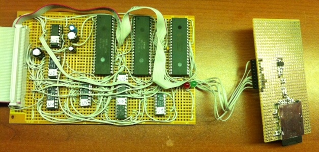
A picture of the ZXpand prototype which I built to verify my circuits.
I have chosen not to use GAL chips to keep the schematic more basic and readable. Somehow I always prefer to use as few custom chips as possible. So I converted the GAL to conventional logic and added some additional circuits to support controlling the second AY chip for 3 more audio channels, which makes a total of 6 channels.
PCB Design
Here you can see a screenshot of the finished PCB layout design. There are many hours that went into this design, including to find new connectors, switches etc, drawing their new PCB shapes, fitting the PCB dimensions and hole positions into a ZX81 case, finalizing the connectivity of the board and at the same time optimizing the power lines and planes. For more perspectives on the PCB, see the component placement picture and the photo of the manufactured PCB further down.
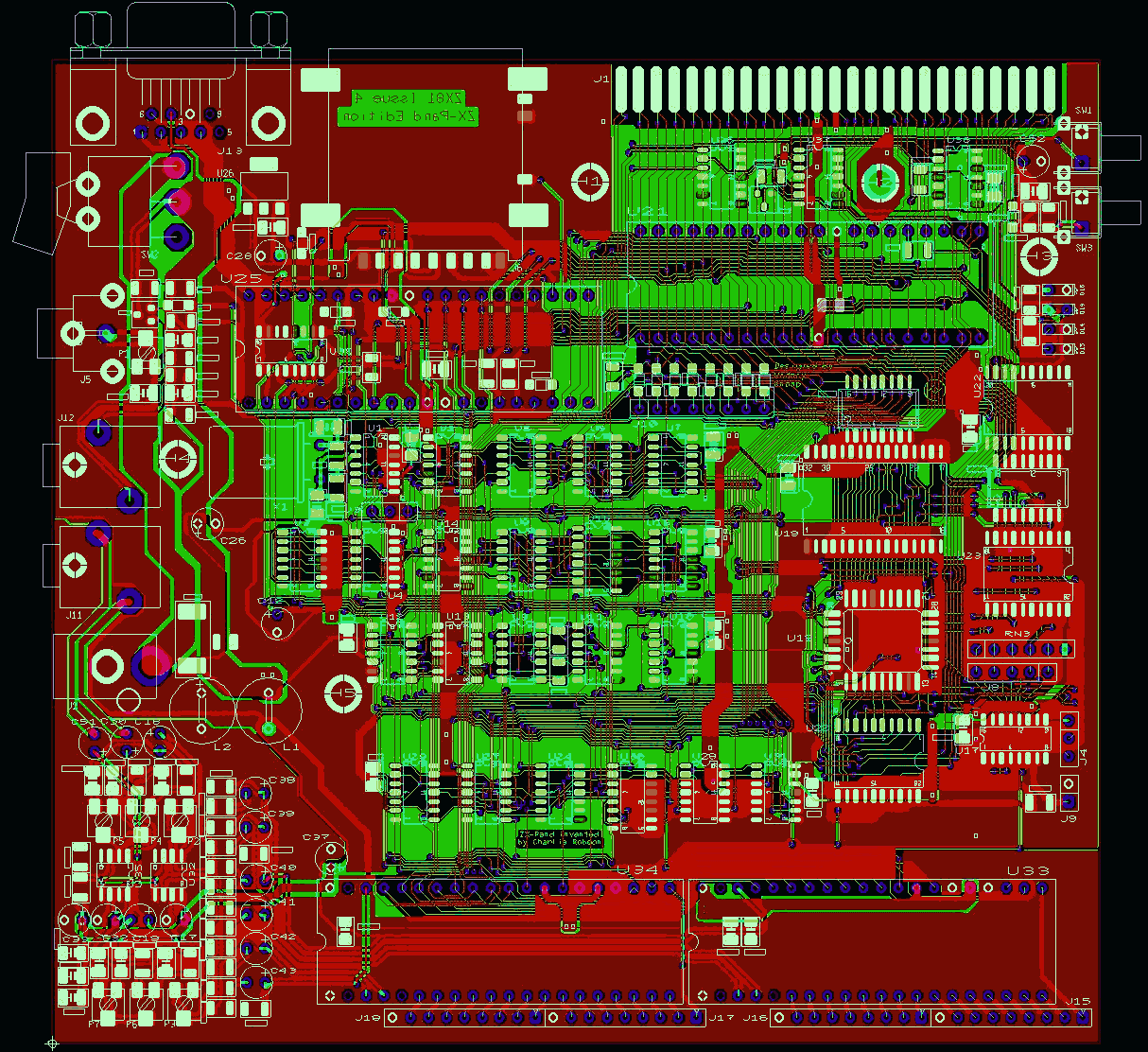
A screenshot of the finished ZX81 Issue 4 ZXpand Edition PCB design.
Component placement
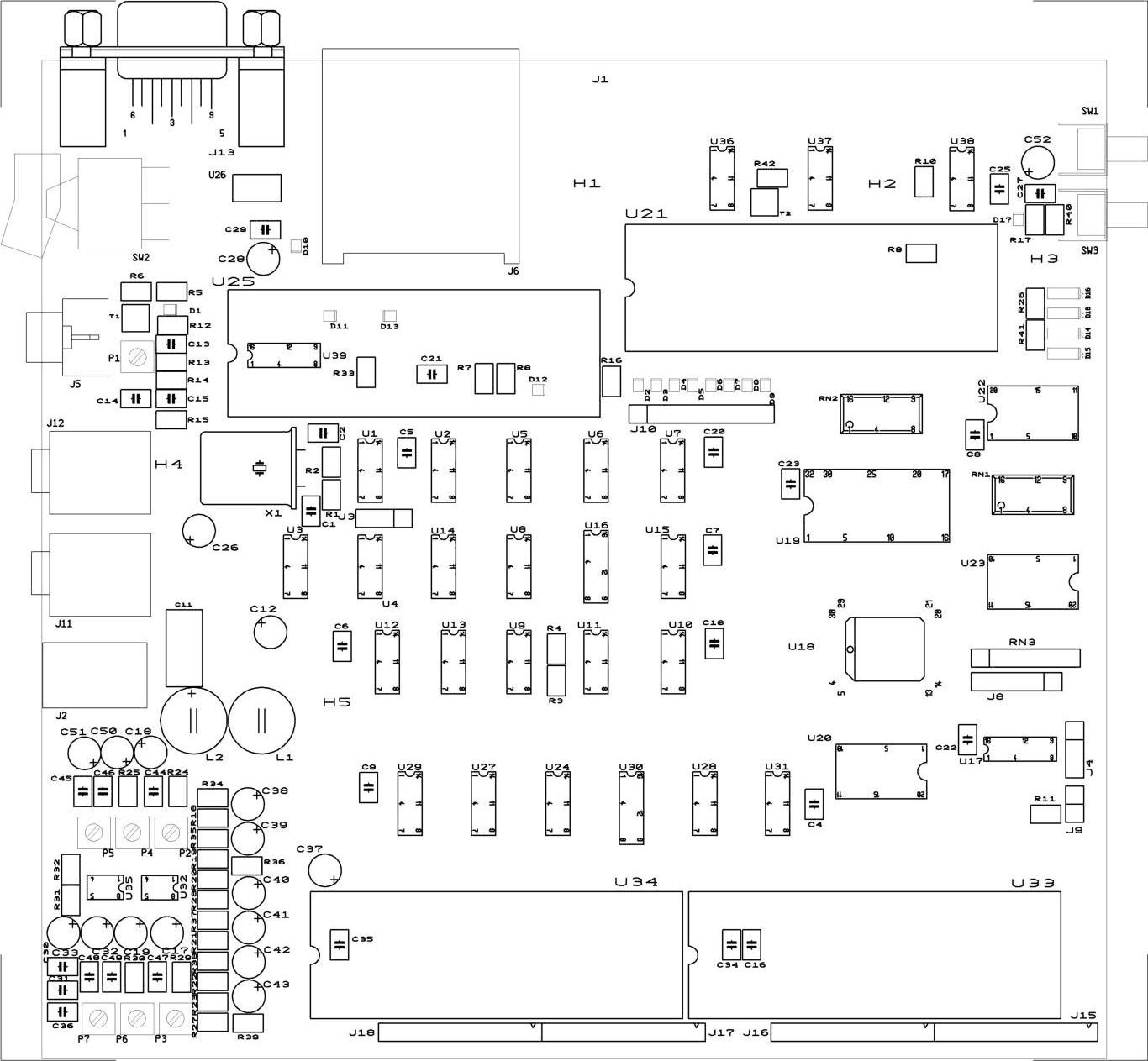
Top layer component placement for the ZX81 Issue 4 ZXpand Edition.
NB. The bottom layer contains two SMD capacitors, both 100nF.
About the expansion connector
The expansion connector is non-ZX81 standard. That means that you will need to make some kind of adapter to attach original ZX81 expansions.
I used this connector layout because it is more conveniant for the PCB design. The expansion connector is based on the Z80 CPU pins, expanded with several important and useful signals from the ZX81 circuits.
From the expansion connector it is easy to:
– make and attach your own external keyboard circuits
– use external ROMs
– attach some sort of color video expansion
– etc.
The video shift register output data is available on the expansion connector, as well as video sync signals, /NOP signal, SH/LD signal, 6.5Mhz video clock, etc. This enables easy experimentation with video expansions which can directly sync to the internal video circuits.
The intended method of connection in my design is to solder a 50pin boxheader in horizontal position directly onto the PCB. I have attempted to make an exact fit in the ZX81 slot based on a boxheader which I use here, but I still need to verify that after I receive the PCB. Into the boxheader you can plug a 50-pin flatcable connector which connects your expansion. This eliminates potential “wobble” contact problems and reduces contact wear. When using a double flatcable connector, if necessary, you could even add more durability to the boxheader on the ZX81 side by leaving the short flatcable assembly inside it, reducing the need to replug on the ZX81 side. It all depends on how often you plan to use expansions and if they frequently need to be changed.
Current project status:
I have sent my design to Beta LAYOUT Ltd. (www.pcb-pool.com). The PCB has been manufactured:
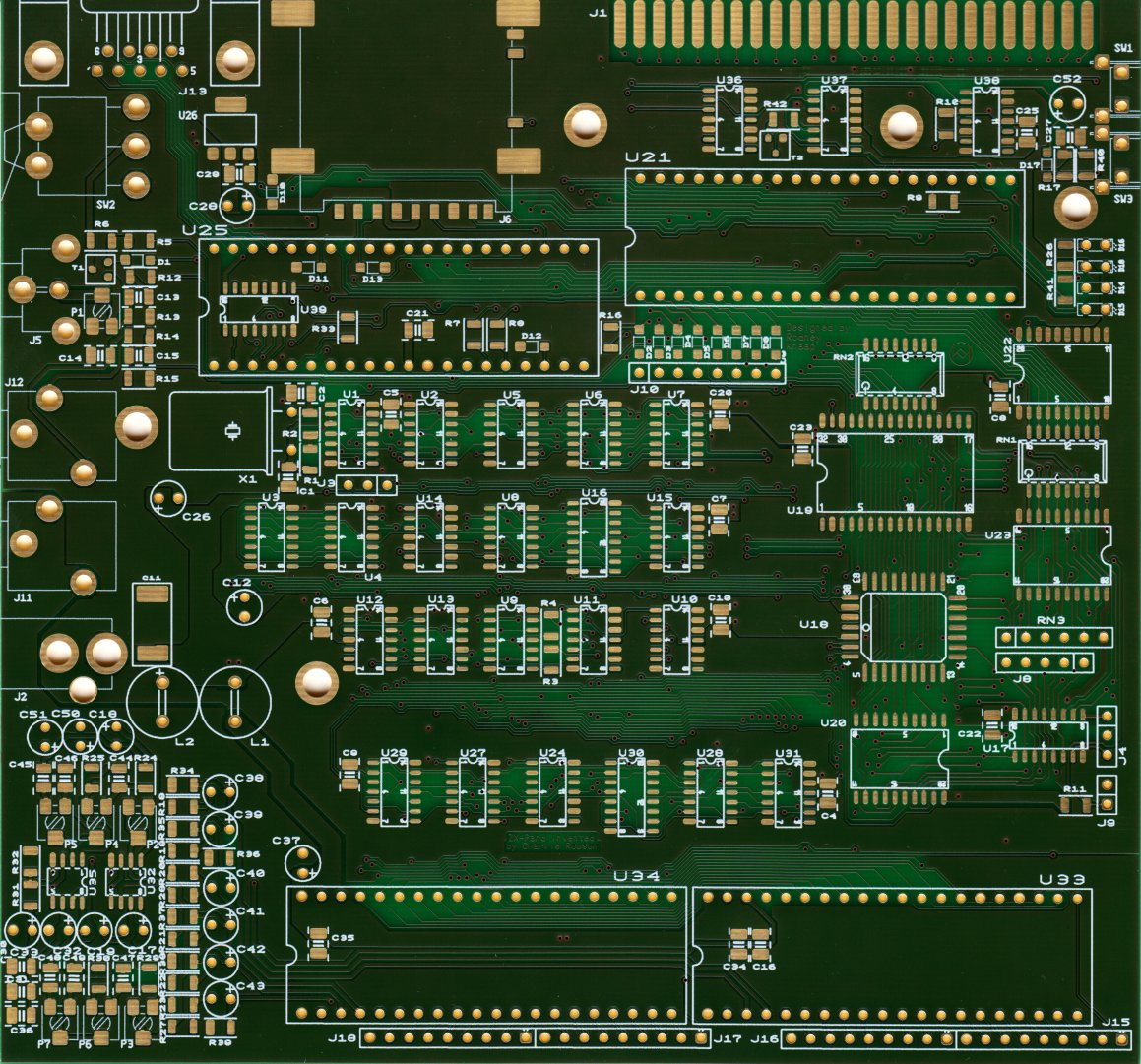
Photo of manufactured PCB.
After fitting the PCB inside the ZX81 case:
– the holes line up with the case screw holes
– connectors all appear to line up properly
– the expansion connector with boxheader will require some work to widen the case opening
– there is enough space above the PCB to accommodate the YM2149 chips, but they should not be socketed to keep a lower profile so the ZX81 case can still be closed properly
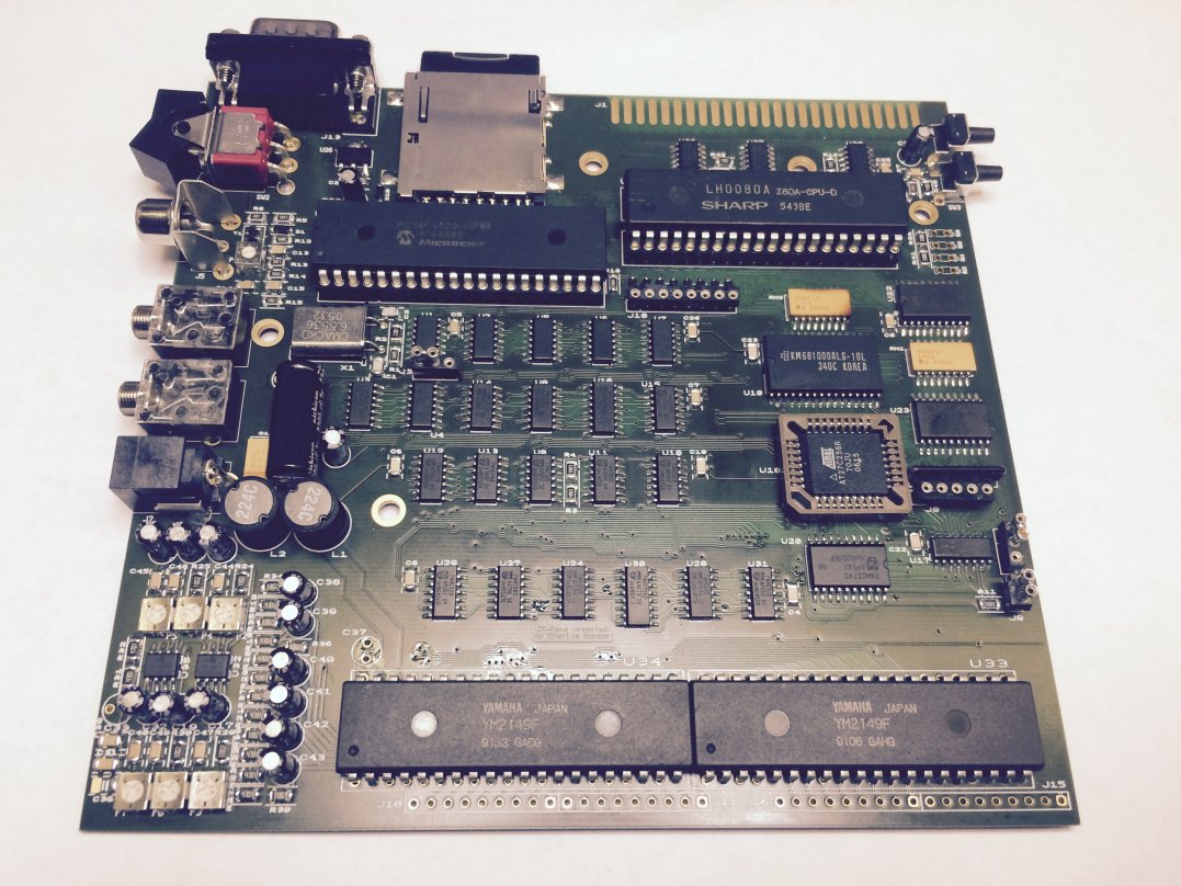
Photo of assembled PCB.
As you can see in the above photo, I have soldered in practically all the components.
Big capacitors will need to be mounted horizontally in the space available. Make sure those capacitors have a small enough diameter.
I have done a hot air reflow and flux removal work of the entire PCB. After that I did some last cleaning with a moist cloth with some alcohol will made the PCB more tidy, almost like from a production.
The photo is not very straight because I used my mobile phone which has a lens that causes this effect.
A few important tips: for example with a 14 pin SMD IC, first solder pins 1 and 8. Mostly these are not power pins and can heat up more easily than for example pin 7 and 14 which connect to wider traces. This allows for easy fixing of the IC to the PCB. Next you can use both hands to solder all other pins. Before doing the rest of the pins, distribute some good quality flux (non-resin) on the pins. This will help you to get a tidy job.
With the SMD resistors, capacitors and transistors, I found the easiest way was to add a very thin layer of solder onto one of the pads. Next position the part with some tweezers, and heat the soldered pad to attach the part onto the PCB. Next solder the older pad(s) and finally solder the first pad.
I have tested all functions of the PCB.
Everything works now. The only thing I am still working on is to further reduce audio power noise.
It is already quite low, but I want to see if it can be improved even further.
The more capacitance on the audio power lines, the lower the power noise in the audio.
The coils separate and filter the audio power from other power area’s, and capacitors can stabilize the power noise behind the coils, that’s the principle I have implemented. The difficult point is to find thin and small capacitors with very high capacitance value.
I will also test with different power supplies, which I expect may also positively impact audio quality.
Mounting the PCB into the ZX81 case
I have made the case openings in my ZX81 case for the joystick connector, power switch, reset and ROM switches, and the SD card slot. I now can close the case with the PCB inside. I used only hand tools to carefully make all the holes after marking their locations into the case plastic. The ZX81 case is made of very good quality plastic which is easy to work on. All connector and switch positions work out nicely with the ZX81 case. After making the required openings I found it didn’t impact the style of the ZX81 much. Part of the locations was fixed due to the height of the PCB, however I feel it worked out well.
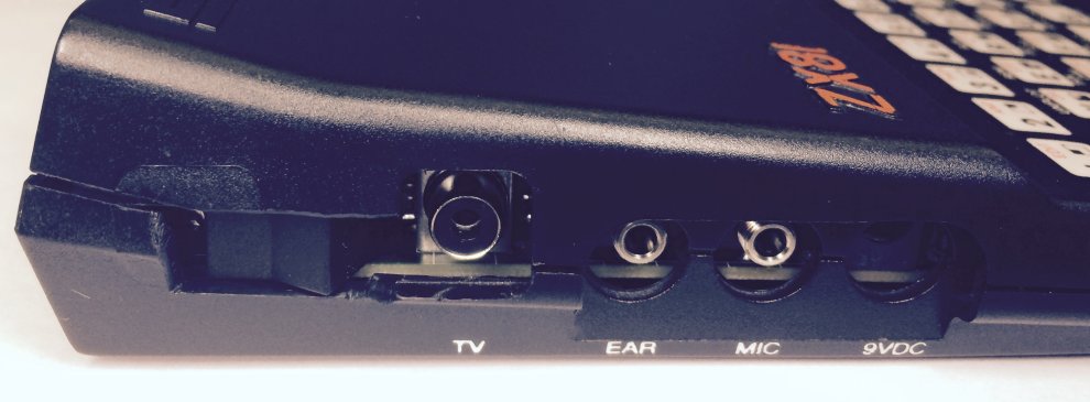
Photo of the left side of the assembled ZX81
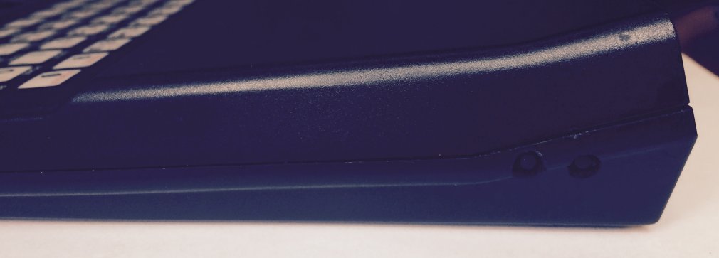
Photo of the right side of the assembled ZX81.
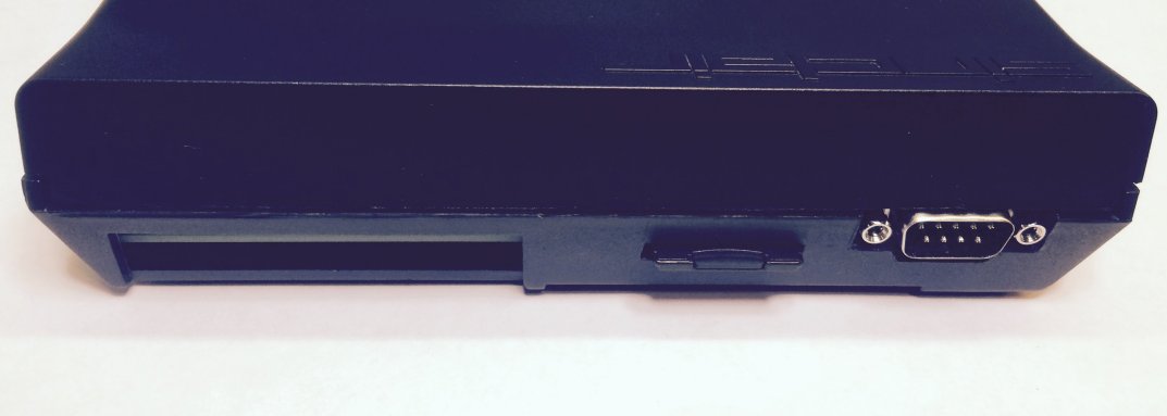
Photo of the rear of the assembled ZX81 with SD card inserted.
Anyone who wants to receive a copy of the files to manufacture a PCB and build this project can contact me, please see the contact page of my website. After you receive the PCB design files, please don’t distribute them to others yourself because after putting so much work into these designs, I would really like to know how many people are interested and find my design useful. If you want to start a batch PCB production as a group of people, please let me know about it, I will be pleased to know it. Anyone can contact me on the email address of this website and I will reply as soon as possible. Remember, this project is non-commercial, only for hobby and home use purposes.
ZXpand was created by Charlie Robson. After finishing my build I will discuss with him how future builders may obtain a programmed ZXpand PIC18F4520 controller in order to use the ZXpand functions. If you are indeed interested in building this project, please read the Building considerations and tips below before starting.
Further things on the to-do list for this project page:
– to add a component list with part numbers of example components.
Example manufacturer part numbers will be helpful to find PDF documentation about connector and switch shapes, dimensions etc.
– to document the audio and tape connectors
Future plans after completing this project
– looking at the Zeddynet LAN adapter created by the German ZX-Team
What I want to do, if my experiments are successful, is to implement the WIZ LAN chip and a few other supporting components directly onto a next PCB design.
– looking at the ZX81 Chroma interface by Paul Farrow
I am thinking about perhaps transferring the Chroma interface chip directly onto a next PCB. I may buy a Chroma interface and experiment with it to see if this could be a viable option. I am not very sure about whether I want to do this yet.
What I really set out to do was to create a very compact single-PCB ZX81 with everything included onboard to make it a lot of fun, stable and very easy to connect and use. In this project, I believe that I have already been succesful to achieve this.
Other ideas for future designs:
– adding a PC keyboard interface
This would enable builders to use some sort of console case and mounting a PC keyboard of their preference in the top of it.
Much like a C64, A1200 or MSX computer.
I plan to create a single-PCB ready-to-use design without any need for add-ons or plugins.
A builder can decide which components to populate onto the board.
I may create a small intermediate PCB design as well, which plugs into the ZX81 Issue 4 – ZXpand Edition expansion connector, and provides LAN, and perhaps, color output.
I hope that this project can be interesting, inspiring, and perhaps useful to other ZX81 enthousiasts who have similar sentiments about the ZX81 as I do. For them I have created this page. I have enjoyed very much to develop and create this design, and it has been a great experience looking back.
Kind regards,
Rodney Knaap
Building considerations and tips
When building this project from a manufactured PCB, it’s a must to consider a few things. After I have built my own PCB, I will elaborate on my experiences and add more tips here.
– Please build this design, only at your own discretion and care. I can’t be held responsible if your ZX81 case suffers some damage or if you encounter any other difficulties or problems, so please first think carefully about everything before attempting this project. Also, this PCB is rather complex so it needs good soldering skills, great care, dedication, requires lots of time and patience, and if necessary, the skill to track down any connection faults and debug your build. All the things involved are completely your own responsibility and you should take this into consideration first before attempting to build this project. I am willing to share the PCB design with you and further tips and experiences that I can think of, but what you do with the information on this page is completely your own decision and your own responsibility.
– The PCB is a quite dense design in order to be able to fit into a tiny ZX81 case. it’s best to first solder in the SMD components. Some SMD components are located underneath DIP parts to save board space. There it needs to be considered that perhaps an IC socket needs to be modified for a better fit on the PCB before soldering it into place.
– use plenty of light and a magnifying glass during your soldering work
– apply a little flux for the SMD parts
– use flux remover after the soldering is finished, be very careful not to get flux into the IC sockets and SD card slot, apply remover accordingly and use a fan to blow away the vapours. Observe all the safety directions of flux remover as this is a flammable liquid and gas. Wear eye protection glasses or magnifying glasses which also can protect your eyes when working on this project.
– LED lights: I suggest to use some attractive shape tiny rectangular LED lights and wire them to the PCB so you can find a good looking position in the ZX81 case. LED positions on the PCB are not meant to be exact LED placements, they are just the connections. The LEDs can benefit from some insulating tape, dark paper, a paint layer or any other darkening material between them to keep their LED light confined and make it very clear which LED is lit. Also, choosing different colour LEDs can be useful to indicate different things. I plan to make the LEDs into a small block which I will fit into the ZX81 case upper shell. If any LED is too bright for your preference, you can use a higher value series resistor to darken it more.
– component holes in the ZX81 case: It will be necessary to make various differently shaped holes into the ZX81 case in order to fit the LEDs, switches, joystick connector and SD memory card slot. Please only build this project in case you actually don’t mind to do this. And take much time to fit and measure everything step by step into the case, and to prepare and do the drilling etc which is necessary. Wear some safety glasses to protect your eyes when drilling and filing etc. I suggest to start with very small holes for proper positioning, and then making them bigger very carefully in order to fit the relevant parts properly.
When drilling holes into the case, hold it tightly on a stable surface so it doesn’t start to spin out of your hands along with the drill’s revolving. When operating a drill, use appropriate drilling speed to make the action more gentle and controllable.
– PCB standoffs of the ZX81 case: because the PCB needed to be very dense, the space around the PCB case mounting holes is limited. It will be necessary to very carefully, slightly modify the ZX81 case standoffs in some places so they can fit onto the PCB’s top side positions around their respective holes. The standoffs have a “+” shape, where near the PCB in some places it will need to be cut slightly to make a smaller “O” shape instead. Some gentle and careful fitting and cutting will certainly be needed. I will include some photo’s of my work on my ZX81 case later to clarify this more.
– membrane keyboard: this keyboard is very delicate and not suitable to directly connect to this PCB. You will need to somehow convert the plastic sheet connections into wired connections without damaging the traces and the plastic sheet material which carries them. In certain cases it may be necessary to change the order of the keyboard connections when wiring them to the PCB. Try to avoid bending or pulling action on the keyboard connection plastics and the conductors on them. In other pages of the hobby area of this website you can see some examples about how I did this type of work. Be careful with what kind of glue you use in order not to chemically damage the keyboard connections with glue solvents. If you use superglue, use some activating spray to reduce influence of glue vapours on the keyboard. Use a ventilator to blow away glue solvent vapour from the keyboard connection plastics and keep the ventilator on the glue work for a long time. Maybe even ventilating it for a day or longer will be better. New keyboard membranes have been available from some websites as I have seen them advertised before. It may still be possible to obtain one, I will report details here if I have done so.
– for SMD soldering, a needle tip soldering iron and very thin 0.35mm soldering tin wire is an absolute must. Using flux can greatly add to the quality of your SMD soldering work. Apply heat effectively in order to reduce soldering time and heat, while at the same time properly letting the soldering tin flow to the right places. Those of you with professional hot air equipment can use a little careful reflow with flux to make the solder properly aligned around the SMD connections and on the PCB pads. Be careful not to melt any soft plastic parts. After finishing the SMD work and carefully cleaning off flux residue from the PCB, inspect every SMD part’s pins for proper electrical connections with a strong magnifying glass.
– fitting the PCB to the case: I have used a lot of care when choosing the part locations. The shape of the ZX81 case makes it slightly difficult to make exact fits until the actual part is in place on the PCB and it’s time to fit and make the holes. I mounted the pcb(not too much force, just enough to keep the PCB in place) with a few screws to fix it and then I marked the locations of the openings onto the case plastic. Do remember to first check and modify all the case standoffs so they can’t damage any components on the PCB.
The copyrights of Sinclair Technology are the property of international computer manufacturer Amstrad. It is not allowed to use any designs provided in this website and/or any Sinclair Technology found elsewhere on the internet for any commercial use. It is not allowed to sell computers built with or based on plans from this website with the intent to make any commercial profit or gain. The sole purpose of the designs in this website is to use the designs for your hobby or for non-commercial learning purposes.
