Introduction
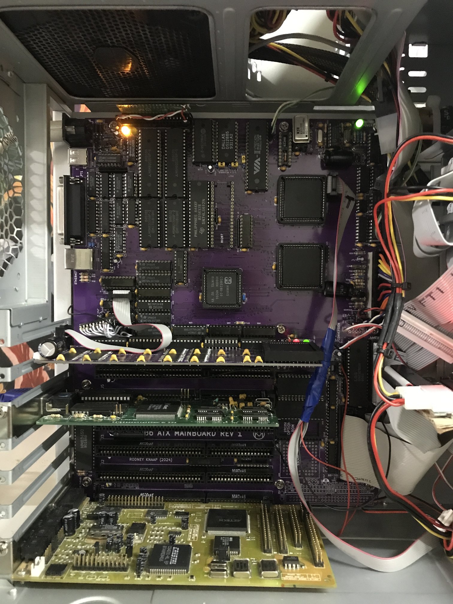
This page describes my design work to develop my own implementation of a 16 bit AT PC system in ATX form factor. The design goal is to create a PC system fully compatible with the industry standard 16 bit AT technology developed by IBM, however to also offer various improvements which will make using such a PC much more easy and in such more enjoyable in my opinion, from a perspective of comfortable and user friendly functionality.
This design, which is now published on my GitHub page, is intended to be used solely and exclusively for retro PC hobby purposes, for retro computing enthousiasts like myself. The design implements a version of logic circuits which is most appealing to me based on my experience with creating mainboard systems while at the same time attempting to keep the system fully compatible with the industry standard 16 bit PC. I have also made various changes and upgrades to the design in order to greatly improve the system beyond the design level of the 5170, which was after all the first AT model. I have made extensive use of CPLDs in order to create the whole design. The amount of logic needed to create the system in the state I wanted was simply not feasible to be done in conventional logic ICs, which would require double or triple the PCB area.
After finishing my XT PC mainboard design project with revision 3, and publishing the designs on GitHub, I started studying the IBM 5170 AT PC circuits, to see if it would be possible to design a 16 bit AT compatible PC in such a way which could be attractive to me. The "secret sauce"-alike AT circuits created by IBM in the 5170 proved to be quite intriguing indeed, the more I studied them. Especially the fact that the AT design is backwards-compatible with XT expansion cards and how IBM implemented this by using the 8 to 16 bit databus translation method. This principle is also supported in part inside the 80286 CPU design itself by Intel. IBM implemented this design in their 16 bit industry PC standard mainboards which started a revolution resulting in very big number of clone designs from various PC manufacturers.
The most interesting variations of AT PC designs from a technical viewpoint to me are the early "discrete chipset" versions, meaning that there actually is no chipset used in the design and that it is fully done in TTL logic and a few PALs and PROM chips. This design method used in the IBM 5170 PC and derived designs by others are particularly interesting because these still can show the interfacing mechanisms in actual logic chips rather than a few highly integrated logic design parts of unknown contents, in the form of one or more PC chipset ICs, which would not at all be interesting for someone like me who is trying to understand how the 16 bit PC/AT actually functions.
Designing my own version of the IBM PC/AT serves to open up various future developments which I will research and explore later on to see what else could be possible to further develop a 16 bit PC system. My AT designs are now published on GitHub and can support clock speeds of up to at least 20MHz.
The most important part of this project is of course the mainboard PCB. In addition I have developed a SRAM memory card to accompany this mainboard. This method provides several advantages:
- saving PCB space which can be used for including more features on the mainboard PCB area
- offering the possibility to upgrade the memory system with faster concepts
The design features:
- dual IDE ports
- HD floppy port
- bidirectional LPT port
- USB mouse to serial conversion using USB and UART concept developed by Limeprogramming
- ATX PSU control
- 7 full size ISA slot connector positions
Phase 1: study of existing designs and finding physical reference hardware examples
I have bought several old example mainboards from the 1980s and found myself initially rather unlucky to come across several unreliable mainboards. The reasons for being unreliable were probably PCB tracks which had become compromised due to the age and previous handling of the mainboards, damage in transport, as well as discovering some poor manufacturing quality such as one particularly badly warped NCR branded PCB, soldered to the ISA slots in pretty warped condition. Straightening such a 4 layer PCB after being mishandled by terrible wave soldering techniques will probably not be an option, especially after the PCB has already proven unreliable.
Anyway, after doing some testing, troubleshooting and repair work on the last mainboards I was lucky enough to come across, I finally now have two reference hardware example mainboards which appear to now be functioning reliably:
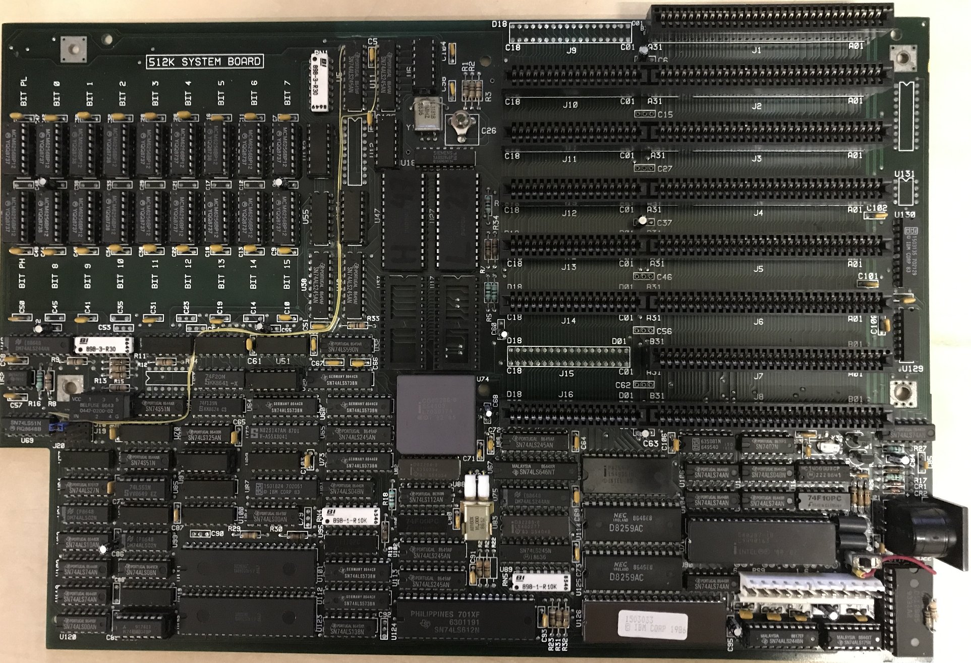
IBM 5170 mainboard "type 3"
The 5170 PC mainboard by IBM which I have studied and repaired is showing particularly beautiful and excellent design and manufacturing quality which I am really delighted with. I found a new appreciation for IBM in those years with respect to design and manufacturing quality after being able to compare between different brands. Though the design I studied contained a small flaw corrected with a few wires, besides this it's really remarkably well made.
The 5170 mainboard was made in two revisions, type 1 which uses smaller capacity DRAMs and a larger form factor square shaped PCB, and type2/3 which implements the same PCB design using a smaller rectangular PCB size as well as larger DRAMs, though unfortunately still only containing 512KB of RAM onboard. Initially I got a lot of RAM parity errors in random areas and the occasional error 107 System Board Error, the so-called "HOT NMI TEST". After desoldering and replacing a few logic ICs which proved to function only marginally, these errors are fully gone from the system.
Next phase: designing and debugging the mainboard and ISA slot memory card
Now that I had a working 5170 I used this as a basis and reference design to design my own advanced new system.
I followed these steps:
- assembling a 100% schematic equivalent of the 5170
- removing the DRAM and decoding logic
- replacing the decoders with CPLDs
- moving most of the AT core logic into the CPLDs
- reverse engineering the U87 system control PAL and adding these circuits to the CPLD
- adding the PC IDE port designs
- adding the floppy disk control design
- adding a UART and the RP2040 interface for the USB mouse
- designing the mainboard PCB and memory card PCB
- designing the initial quartus projects for the CPLDs
- sending the mainboard and memory card PCB designs to JLCPCB for manufacturing
- getting the parts needed such as the CPLDs and PLCC sockets
- assembling the system
- debugging the timing inside the System controller CPLD design
- debugging all the system functions inside the CPLDs
- developing replacement control logic for replacing the 82284 and 82288 chips
- removing the 82284 and 82288 from the PCB and rewiring the control
- developing a shadow RAM system
- developing assembly code to make and enable the shadow copy before system init
- optimizing the system control timing to support higher clock speeds
- upgrading logic types of transceivers and latches in the system
- testing and debugging the highest clock speed, so far at 20MHz CPU clock
- optimizing the CPLD pin usage and reducing a lot of inputs which I was then able to test
- updating the full features into a revised PCB design (in progress)
You can also read my project thread on the VCF forums which has all the design details documented and described chronologically.

Mouse control
While testing varous 286 and 386 mainboards, I noticed that mouse control particularly in Windows was not ideal. I was using a serial ball mouse since these PCs don't feature a PS/2 mouse port. For this new project I have done some research to see what the alternatives could be for a serial mouse.
The best solution so far is the USB to serial mouse adapter project by GitHub user LimeProgramming.
Adam has created an excellent open source project using the RP2040 controller on a Raspberry Pi Pico PCB. The RP2040 controller, though arguably having even more processing power than a 286, is a cheap small device which conveniently offers USB port capability which was used in his GitHub project to interface with the USB mouse.
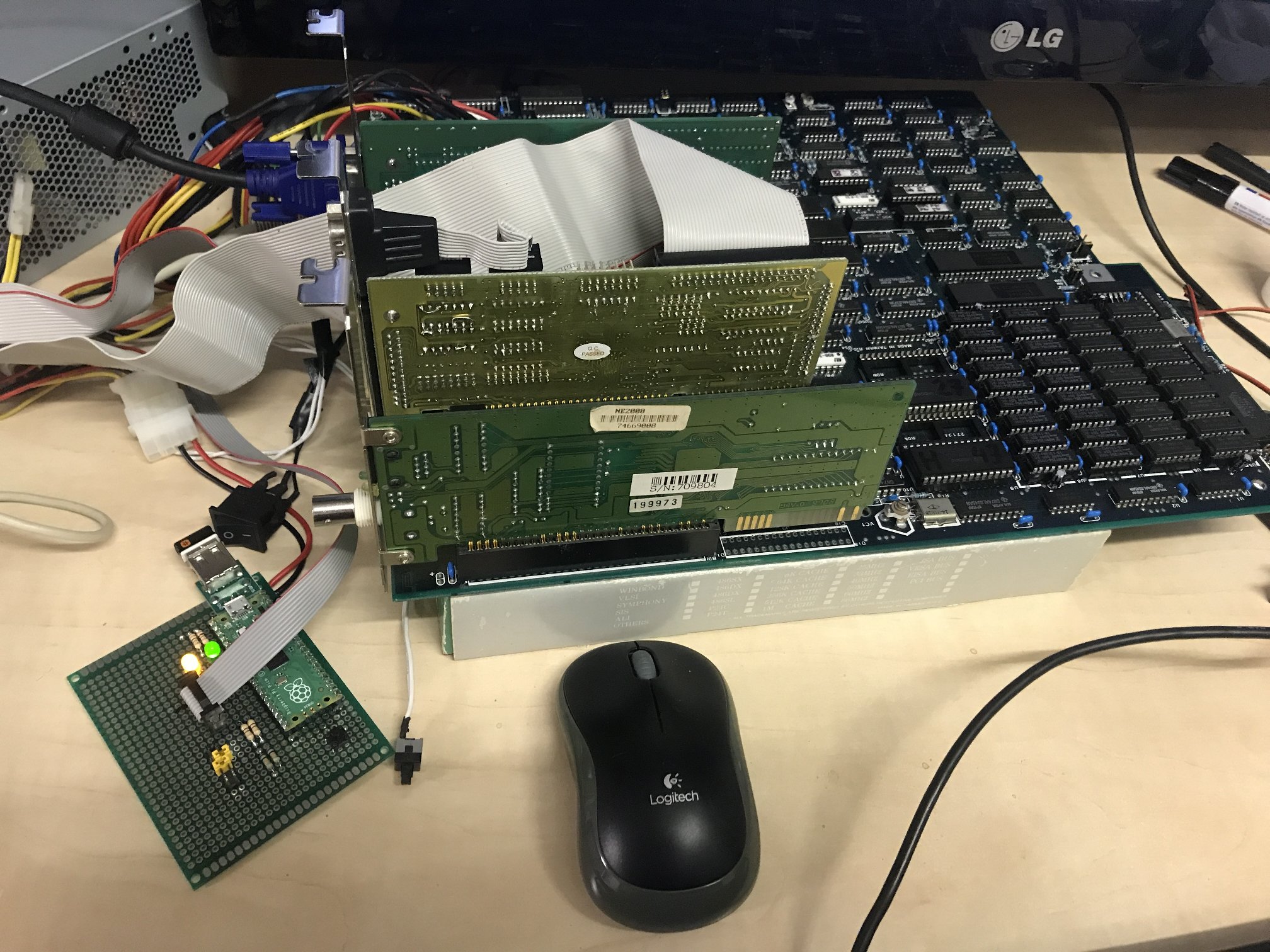
I have built a simplified prototype wired up version of the USB to serial mouse adapter and tested it with my 286 mainboard via a modified multi I/O card where I removed the +/- 12V level converters and plugged my prototype board directly onto the COM2 header and I can report that it works perfectly with my Logitech USB wireless mouse. The mouse pointer travel speed can be configured by two jumpers which is sufficient to achieve a really great result using 640x480 VGA resolution in Windows. This excellent solution by Adam is a definate keeper from now on!
I will integrate a simplified version of Adams project in my new 286 mainboard design, which will feature a USB connector in the I/O shield area for using a modern USB mouse. The RP2040 will be featured on a small plug in PCB which will sit vertically in relation to the mainboard on a small header to reduce the footprint size necessary on my mainboard PCB layout. I may try to use a stamp sized version of a RP2040 PCB on a plugin PCB which would be the smallest solution other than soldering the RP2040 components directly which are rather tiny compared to other components on the mainboard. The serial mouse data will be passed to a regular COM2 UART chip using TTL level serial connections with the RP2040, omitting the +/-12V RS232 logic. The code in the RP2040 flash will be the original code as featured in Adams project which suits my mainboard perfectly.
As you can see in the project photo, the system has been extensively upgraded and modified. So I am working on a upgraded PCB design to reflect all the changes and test results.
I am also in the research/concept phase of developing my next FPGA based system which will feature a 486 PC based initially on a 486DX CPU running in 16 bit mode, and later will evolve into a full 32 bit system. The system will feature FPGA technology which will also provide memory control and fast modern RAM for the system.
In the next project design, I will be using a modular concept which means that different areas of the system will be featured on separate modules which can be replaced with future upgrades as the design evolves and changes. One of the modules will be featuring the CPU, so that the mainboard can remain the same throughout several design revisions, even when using a faster generation CPU. Eventually the system will evolve into using Vesa Local Bus or PCI based technology, or possibly I will explore both of these in that order. It also depends on the specifications and complexity of what would be needed if this is feasible for me to include into the system, and of course on whether the design specifications for these upgrades are openly available.
Please see my GitHub page and my VCF Forum thread for the latest full design details.
On the GitHub page I have also included a list of all the people who contributed ideas and helped to inspire the project.
I thank everyone who has contributed to the project!
Please check out the GitHub for the full details.
Last updated: october 5th, 2024.

